General / Topics
G7 Practical Circuits
G7 Practical Circuits (General questions)38 questions in 3 groups. The exam asks 3 questions from this topic, one from each group.
G7A Power supplies; schematic symbols
G7A01
What is the function of a power supply bleeder resistor?
- A. It acts as a fuse for excess voltage
- B. It discharges the filter capacitors when power is removed
- C. It removes shock hazards from the induction coils
- D. It eliminates ground loop current
Show answer
B. It discharges the filter capacitors when power is removed
Filter capacitors in a power supply can hold a dangerous charge after the supply is switched off. A bleeder resistor connected across them slowly drains that charge, reducing the shock hazard during servicing.
- A. A fuse protects against excess current by opening the circuit; a bleeder resistor carries a small steady current and does not limit voltage.
- C. The shock hazard that remains after power is removed is the charge stored in the filter capacitors, which is what the bleeder resistor drains, not anything stored in coils.
- D. Ground loop current is reduced by proper bonding and wiring layout; a bleeder resistor does not affect it.
G7A02
Which of the following components are used in a power supply filter network?
- A. Diodes
- B. Transformers and transducers
- C. Capacitors and inductors
- D. All these choices are correct
Show answer
C. Capacitors and inductors
A power supply filter smooths the pulsating output of the rectifier into steady DC. Capacitors store charge and fill in between the peaks, and inductors (chokes) oppose changes in current; together they reduce ripple.
- A. Diodes form the rectifier, which converts AC to pulsating DC ahead of the filter; they do not smooth ripple.
- B. Transformers change AC voltage levels, and transducers convert energy from one form to another; neither smooths ripple.
- D. Diodes, transformers and transducers are not filter components, so not all the choices are correct.
G7A03
Which type of rectifier circuit uses two diodes and a center-tapped transformer?
- A. Full-wave
- B. Full-wave bridge
- C. Half-wave
- D. Synchronous
Show answer
A. Full-wave
A full-wave center-tap rectifier uses two diodes, one at each end of a center-tapped secondary winding. Each diode conducts on alternate half cycles, so both halves of the AC cycle reach the load.
- B. A full-wave bridge rectifier uses four diodes and does not need a center-tapped transformer.
- C. A half-wave rectifier uses a single diode and passes only one half of each cycle.
- D. A synchronous rectifier uses transistors switched in step with the AC in place of diodes; it is not defined by two diodes and a center tap.
G7A04
What is characteristic of a half-wave rectifier in a power supply?
- A. Only one diode is required
- B. The ripple frequency is twice that of a full-wave rectifier
- C. More current can be drawn from the half-wave rectifier
- D. The output voltage is two times the peak input voltage
Show answer
A. Only one diode is required
A half-wave rectifier needs only one diode, which passes one half of each AC cycle and blocks the other half.
- B. A half-wave rectifier's ripple frequency equals the AC input frequency, which is half that of a full-wave rectifier, not twice.
- C. A half-wave rectifier uses only half of each cycle, so it delivers less output for a given transformer, not more.
- D. An output of twice the peak input voltage describes a voltage doubler, not a half-wave rectifier.
G7A05
What portion of the AC cycle is converted to DC by a half-wave rectifier?
- A. 90 degrees
- B. 180 degrees
- C. 270 degrees
- D. 360 degrees
Show answer
B. 180 degrees
A full AC cycle is 360 degrees. A half-wave rectifier conducts during only one half of each cycle, which is 180 degrees.
- A. 90 degrees is a quarter cycle; a half-wave rectifier conducts for a full half cycle.
- C. 270 degrees is three quarters of a cycle; a half-wave rectifier conducts for only half.
- D. 360 degrees, the whole cycle, is converted by a full-wave rectifier, not a half-wave one.
G7A06
What portion of the AC cycle is converted to DC by a full-wave rectifier?
- A. 90 degrees
- B. 180 degrees
- C. 270 degrees
- D. 360 degrees
Show answer
D. 360 degrees
A full-wave rectifier steers both halves of each AC cycle to the load with the same polarity, so the whole 360-degree cycle is converted to pulsating DC.
- A. 90 degrees is a quarter cycle; a full-wave rectifier uses the whole cycle.
- B. 180 degrees, half the cycle, is what a half-wave rectifier converts.
- C. 270 degrees is three quarters of a cycle; a full-wave rectifier uses both halves, the full 360 degrees.
G7A07
What is the output waveform of an unfiltered full-wave rectifier connected to a resistive load?
- A. A series of DC pulses at twice the frequency of the AC input
- B. A series of DC pulses at the same frequency as the AC input
- C. A sine wave at half the frequency of the AC input
- D. A steady DC voltage
Show answer
A. A series of DC pulses at twice the frequency of the AC input
A full-wave rectifier turns each half cycle of the input into a pulse of the same polarity, so there are two pulses per AC cycle. A 60 Hz input produces 120 DC pulses per second.
- B. Pulses at the same frequency as the AC input come from a half-wave rectifier, which uses only one half of each cycle.
- C. A rectifier's output does not reverse polarity, so it is not a sine wave, and its pulse rate is twice the input frequency, not half.
- D. A steady DC voltage requires a filter after the rectifier; the unfiltered output is a series of pulses.
G7A08
Which of the following is characteristic of a switchmode power supply as compared to a linear power supply?
- A. Faster switching time makes higher output voltage possible
- B. Fewer circuit components are required
- C. High-frequency operation allows the use of smaller components
- D. Inherently more stable
Show answer
C. High-frequency operation allows the use of smaller components
A switchmode supply switches at frequencies far above the 60 Hz power line, often tens or hundreds of kilohertz. At those frequencies, transformers, inductors and filter capacitors can be much smaller and lighter, so the supply is compact.
- A. Output voltage is set by the circuit design and control loop, not by switching speed, and linear supplies can also produce high voltages.
- B. A switchmode supply typically needs more components than a linear supply, including a controller, switching transistors and extra filtering.
- D. A switchmode supply depends on a feedback loop that must be designed carefully to be stable; stability is not an inherent advantage over a linear supply.
G7A09
Which symbol in figure G7-1 represents a field effect transistor?
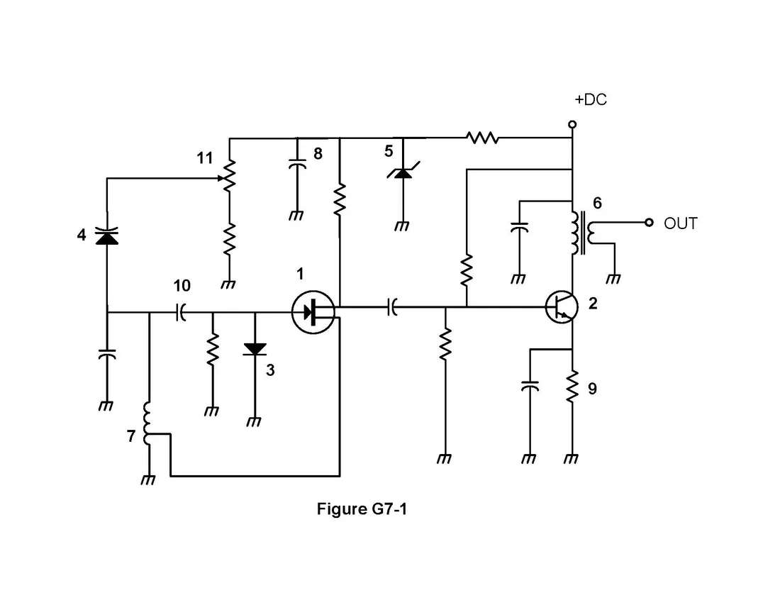
Figure G7-1 - A. Symbol 2
- B. Symbol 5
- C. Symbol 1
- D. Symbol 4
Show answer
C. Symbol 1
Symbol 1 is a junction field-effect transistor (FET): a circle containing a vertical bar for the channel, with drain and source leads at the bar and a gate lead whose arrow points at the channel.
- A. Symbol 2 is an NPN bipolar junction transistor, with an angled emitter lead whose arrow points outward.
- B. Symbol 5 is a Zener diode, a diode symbol whose bar has bent ends.
- D. Symbol 4 is a varactor (variable-capacitance diode), a diode symbol combined with a curved capacitor plate.
G7A10
Which symbol in figure G7-1 represents a Zener diode?
Figure G7-1 - A. Symbol 4
- B. Symbol 1
- C. Symbol 11
- D. Symbol 5
Show answer
D. Symbol 5
Symbol 5 is a Zener diode: a triangle pointing to a bar whose ends are bent, forming a Z shape. In the figure it connects to ground from a supply line fed through a series resistor, the usual way a Zener diode holds a steady voltage.
- A. Symbol 4 is a varactor, a diode whose capacitance changes with reverse voltage; its symbol adds a curved capacitor plate to the diode.
- B. Symbol 1 is a junction field-effect transistor.
- C. Symbol 11 is a potentiometer: a resistor zigzag with an arrow for the adjustable wiper.
G7A11
Which symbol in figure G7-1 represents an NPN junction transistor?
Figure G7-1 - A. Symbol 1
- B. Symbol 2
- C. Symbol 7
- D. Symbol 11
Show answer
B. Symbol 2
Symbol 2 is an NPN bipolar junction transistor: a circle with a bar for the base and two angled leads for collector and emitter, with the arrow on the emitter pointing outward, away from the base. In a PNP transistor, the arrow points inward.
- A. Symbol 1 is a junction field-effect transistor, with a channel bar and an arrow on the gate lead.
- C. Symbol 7 is a tapped inductor: a coil with a connection partway along it.
- D. Symbol 11 is a potentiometer: a resistor with an adjustable wiper arrow.
G7A12
Which symbol in Figure G7-1 represents a solid core transformer?
Figure G7-1 - A. Symbol 4
- B. Symbol 7
- C. Symbol 6
- D. Symbol 1
Show answer
C. Symbol 6
Symbol 6 is a transformer: two coils side by side with parallel straight lines between them. The straight lines show a solid magnetic core; an air-core transformer is drawn without them.
- A. Symbol 4 is a varactor, a diode whose capacitance changes with applied voltage.
- B. Symbol 7 is a single coil with a tap, an inductor rather than a transformer with two windings.
- D. Symbol 1 is a junction field-effect transistor.
G7A13
Which symbol in Figure G7-1 represents a tapped inductor?
Figure G7-1 - A. Symbol 7
- B. Symbol 11
- C. Symbol 6
- D. Symbol 1
Show answer
A. Symbol 7
Symbol 7 is a tapped inductor: a single coil drawn as a series of loops, with an extra connection partway along the winding. In the figure, the tap connects to the field-effect transistor at symbol 1.
- B. Symbol 11 is a potentiometer: a resistor with an adjustable wiper arrow.
- C. Symbol 6 is a transformer with two separate windings on a solid core.
- D. Symbol 1 is a junction field-effect transistor.
G7B Digital circuits; amplifiers and oscillators
G7B01
What is the purpose of neutralizing an amplifier?
- A. To limit the modulation index
- B. To eliminate self-oscillations
- C. To cut off the final amplifier during standby periods
- D. To keep the carrier on frequency
Show answer
B. To eliminate self-oscillations
Capacitance inside an amplifying device, such as grid-to-plate capacitance in a tube, feeds some of the output back to the input and can make an RF amplifier oscillate on its own. Neutralizing adds an equal feedback path of opposite phase that cancels it, eliminating self-oscillation.
- A. Modulation index is set by the modulating signal and the modulator; neutralization does not limit it.
- C. Cutting off a final amplifier during standby is done with bias or switching, not neutralization.
- D. Carrier frequency is set by the oscillator and frequency control circuits; neutralization stabilizes the amplifier, not the frequency.
G7B02
Which of these classes of amplifiers has the highest efficiency?
- A. Class A
- B. Class B
- C. Class AB
- D. Class C
Show answer
D. Class C
An amplifier's efficiency rises as its amplifying device conducts for less of each cycle. A Class C amplifier conducts for less than half the cycle, so it wastes less power as heat than Class A, AB or B, at the cost of distorting the waveform.
- A. Class A conducts for the whole cycle and has the lowest efficiency of these classes, with a theoretical maximum of 50 percent.
- B. Class B conducts for half the cycle and is more efficient than Class A, but less efficient than Class C.
- C. Class AB conducts for more than half the cycle, so its efficiency falls between Class A and Class B.
G7B03
Which of the following describes the function of a two-input AND gate?
- A. Output is high when either or both inputs are low
- B. Output is high only when both inputs are high
- C. Output is low when either or both inputs are high
- D. Output is low only when both inputs are high
Show answer
B. Output is high only when both inputs are high
An AND gate's output is high only when all its inputs are high. For a two-input AND gate, if either input is low, the output is low.
- A. Output high when either or both inputs are low describes a NAND gate, the inverse of AND.
- C. Output low when either or both inputs are high describes a NOR gate.
- D. Output low only when both inputs are high also describes a NAND gate, the inverse of AND.
G7B04
In a Class A amplifier, what percentage of the time does the amplifying device conduct?
- A. 100%
- B. More than 50% but less than 100%
- C. 50%
- D. Less than 50%
Show answer
A. 100%
A Class A amplifier is biased so the amplifying device conducts during the entire input cycle, 100 percent of the time. This gives low distortion but low efficiency.
- B. Conduction for more than 50 but less than 100 percent of the cycle defines Class AB.
- C. Conduction for 50 percent of the cycle, one half cycle, defines Class B.
- D. Conduction for less than 50 percent of the cycle defines Class C.
G7B05
How many states does a 3-bit binary counter have?
- A. 3
- B. 6
- C. 8
- D. 16
Show answer
C. 8
Each bit has two possible states, so the number of states doubles with each bit added. A 3-bit counter has 2 x 2 x 2 = 8 states, counting from 000 to 111 in binary (0 to 7).
- A. 3 is the number of bits, not the number of states they can represent.
- B. 6 is 2 x 3; the number of states is 2 multiplied by itself 3 times, which is 8.
- D. 16 is the number of states of a 4-bit counter (2 x 2 x 2 x 2).
G7B06
What is a shift register?
- A. A clocked array of circuits that passes data in steps along the array
- B. An array of operational amplifiers used for tri-state arithmetic operations
- C. A digital mixer
- D. An analog mixer
Show answer
A. A clocked array of circuits that passes data in steps along the array
A shift register is a chain of flip-flops driven by a common clock. On each clock pulse, every stored bit moves one position along the chain, so data passes through the array in steps.
- B. Shift registers are digital circuits built from flip-flops, not arrays of operational amplifiers.
- C. A mixer combines signals to produce new frequencies; a shift register stores bits and moves them along in steps.
- D. An analog mixer combines signals to produce sum and difference frequencies; a shift register is a digital storage circuit.
G7B07
Which of the following are basic components of a sine wave oscillator?
- A. An amplifier and a divider
- B. A frequency multiplier and a mixer
- C. A circulator and a filter operating in a feed-forward loop
- D. A filter and an amplifier operating in a feedback loop
Show answer
D. A filter and an amplifier operating in a feedback loop
An oscillator is an amplifier with positive feedback: part of its output returns to its input in phase. A filter in the feedback loop, such as an LC tank or a crystal, allows this only at one frequency, producing a sine wave.
- A. A divider lowers the frequency of a signal that already exists; an amplifier and a divider have no feedback path to sustain oscillation.
- B. Frequency multipliers and mixers convert existing signals to new frequencies; they do not create oscillation.
- C. A circulator routes RF between ports, and a feed-forward path does not return the output to the input, so this arrangement cannot sustain oscillation.
G7B08
How is the efficiency of an RF power amplifier determined?
- A. Divide the DC input power by the DC output power
- B. Divide the RF output power by the DC input power
- C. Multiply the RF input power by the reciprocal of the RF output power
- D. Add the RF input power to the DC output power
Show answer
B. Divide the RF output power by the DC input power
Efficiency compares the useful output to the power drawn from the supply: efficiency = RF output power / DC input power. For example, 100 W of RF output from 200 W of DC input is 50 percent efficient.
- A. An RF power amplifier's output is RF, not DC, and dividing input by output would give the inverse of efficiency.
- C. RF input multiplied by the reciprocal of RF output is RF input / RF output, the inverse of power gain, not efficiency.
- D. Adding two powers does not produce a ratio, and an RF amplifier has no DC output.
G7B09
What determines the frequency of an LC oscillator?
- A. The number of stages in the counter
- B. The number of stages in the divider
- C. The inductance and capacitance in the tank circuit
- D. The time delay of the lag circuit
Show answer
C. The inductance and capacitance in the tank circuit
An LC oscillator runs at the resonant frequency of its tank circuit, f = 1 / (2 x π x square root of (L x C)). Increasing either the inductance or the capacitance lowers the frequency.
- A. Counter stages count pulses in digital circuits; they do not set the frequency of an LC oscillator.
- B. Divider stages produce lower frequencies from an existing signal; an LC oscillator's frequency comes from its tank circuit.
- D. Phase shift or delay in resistor-capacitor networks sets the frequency of RC oscillators, not LC oscillators.
G7B10
Which of the following describes a linear amplifier?
- A. Any RF power amplifier used in conjunction with an amateur transceiver
- B. An amplifier in which the output preserves the input waveform
- C. A Class C high efficiency amplifier
- D. An amplifier used as a frequency multiplier
Show answer
B. An amplifier in which the output preserves the input waveform
A linear amplifier produces a larger copy of its input with the same waveform shape. That is needed for signals whose amplitude carries information, such as SSB and AM.
- A. Amateurs often call any external power amplifier a linear, but the term describes how faithfully the output follows the input, not how the amplifier is connected.
- C. A Class C amplifier distorts the waveform heavily, so it is not linear.
- D. A frequency multiplier is deliberately nonlinear so that it generates harmonics.
G7B11
For which of the following modes is a Class C power stage appropriate for amplifying a modulated signal?
- A. SSB
- B. FM
- C. AM
- D. All these choices are correct
Show answer
B. FM
FM carries its information in frequency changes and has a constant amplitude, so the waveform distortion of a Class C stage does not harm it. Output filtering removes the harmonics, and Class C provides high efficiency.
- A. SSB carries information in amplitude changes, so a Class C stage would distort it; SSB needs a linear amplifier.
- C. An AM signal carries information in its amplitude, so once modulated it needs a linear amplifier; a Class C stage would distort the envelope.
- D. Only FM tolerates Class C amplification; SSB and AM do not, so not all the choices are correct.
G7C Transceiver design; filters; oscillators; digital signal processing (DSP)
G7C01
What circuit is used to select one of the sidebands from a balanced modulator?
- A. Carrier oscillator
- B. Filter
- C. IF amplifier
- D. RF amplifier
Show answer
B. Filter
A balanced modulator produces a double-sideband signal with the carrier suppressed. A narrow filter, often a crystal filter, then passes one sideband and rejects the other, producing single sideband.
- A. The carrier oscillator supplies the carrier signal to the balanced modulator; it does not remove a sideband.
- C. An IF amplifier increases signal strength but does not choose between sidebands.
- D. An RF amplifier increases signal strength but does not choose between sidebands.
G7C02
What output is produced by a balanced modulator?
- A. Frequency modulated RF
- B. Audio with equalized frequency response
- C. Audio extracted from the modulation signal
- D. Double-sideband modulated RF
Show answer
D. Double-sideband modulated RF
A balanced modulator mixes the audio with the carrier and cancels the carrier itself, leaving both sidebands: double-sideband, suppressed-carrier RF. A filter can then remove one sideband to make SSB.
- A. A balanced modulator produces amplitude sidebands, not frequency modulation.
- B. Equalizing audio frequency response is the job of an audio equalizer, not a modulator.
- C. Extracting audio from a modulated signal is demodulation, done by a detector in a receiver.
G7C03
What is one reason to use an impedance matching transformer at a transmitter output?
- A. To minimize transmitter power output
- B. To present the desired impedance to the transmitter and feed line
- C. To reduce power supply ripple
- D. To minimize radiation resistance
Show answer
B. To present the desired impedance to the transmitter and feed line
A transmitter delivers its rated power properly only into the load impedance it is designed for, usually 50 ohms. An impedance matching transformer converts the feed line or antenna impedance so that the transmitter and feed line each see the impedance they need.
- A. Matching lets the transmitter deliver its full power; it is not used to minimize power output.
- C. Power supply ripple is reduced by filter capacitors and inductors in the supply, not by a transformer at the transmitter output.
- D. Radiation resistance is a property of the antenna; a matching transformer at the transmitter does not set it, and reducing it would not help.
G7C04
How is a product detector used?
- A. Used in test gear to detect spurious mixing products
- B. Used in a transmitter to perform frequency multiplication
- C. Used in an FM receiver to filter out unwanted sidebands
- D. Used in a single sideband receiver to extract the modulated signal
Show answer
D. Used in a single sideband receiver to extract the modulated signal
A product detector mixes the incoming signal with a signal from a local oscillator, often called the beat frequency oscillator. The difference product recovers the audio from SSB and CW signals, which lack the carrier that an AM envelope detector needs.
- A. Spurious mixing products are measured with test equipment such as a spectrum analyzer; a product detector is a receiver demodulator.
- B. Frequency multiplication is done by a multiplier stage that generates harmonics, not by a product detector.
- C. FM receivers use a discriminator or other FM detector; a product detector is used for SSB and CW.
G7C05
Which of the following is characteristic of a direct digital synthesizer (DDS)?
- A. Extremely narrow tuning range
- B. Relatively high-power output
- C. Pure sine wave output
- D. Variable output frequency with the stability of a crystal oscillator
Show answer
D. Variable output frequency with the stability of a crystal oscillator
A direct digital synthesizer generates a waveform by stepping through stored sine wave values and feeding them to a digital-to-analog converter, clocked by a crystal reference oscillator. Its output frequency can be set in fine steps over a wide range, with the stability of the crystal reference.
- A. A DDS has a wide tuning range, set by changing a digital value, not an extremely narrow one.
- B. A DDS is a low-level signal source; later stages amplify its output.
- C. A DDS output is built from digital steps and contains spurious signals, so it needs filtering and is not a pure sine wave.
G7C06
Which of the following is an advantage of a digital signal processing (DSP) filter compared to an analog filter?
- A. A wide range of filter bandwidths and shapes can be created
- B. Fewer digital components are required
- C. Mixing products are greatly reduced
- D. The DSP filter is much more effective at VHF frequencies
Show answer
A. A wide range of filter bandwidths and shapes can be created
A DSP filter is a set of calculations performed on a digitized signal, so changing its bandwidth or shape only requires changing the numbers. One DSP system can provide many filter bandwidths and shapes that would each need separate hardware in an analog design.
- B. A DSP filter needs analog-to-digital and digital-to-analog conversion plus a processor, so it does not reduce the number of digital components.
- C. Mixing products come from mixers and other nonlinear stages; a DSP filter does not reduce them.
- D. DSP filters typically work on audio or a low intermediate frequency; their advantage is flexibility, not effectiveness at VHF.
G7C07
What term specifies a filter’s attenuation inside its passband?
- A. Insertion loss
- B. Return loss
- C. Q
- D. Ultimate rejection
Show answer
A. Insertion loss
Insertion loss is the attenuation a filter causes to signals within its passband, the signals it is meant to pass. A good filter has low insertion loss.
- B. Return loss measures how much power is reflected back because of a mismatch, not attenuation within the passband.
- C. Q describes the sharpness or selectivity of a resonant circuit or filter, not its passband loss.
- D. Ultimate rejection is the maximum attenuation of signals outside the passband, not attenuation inside it.
G7C08
Which parameter affects receiver sensitivity?
- A. Input amplifier gain
- B. Demodulator stage bandwidth
- C. Input amplifier noise figure
- D. All these choices are correct
Show answer
D. All these choices are correct
Receiver sensitivity is the weakest signal the receiver can detect above its own noise. The input amplifier's noise figure, its gain (which reduces the effect of noise from later stages) and the bandwidth at the demodulator (narrower bandwidth admits less noise) all affect it.
- A. Input amplifier gain does affect sensitivity by reducing the effect of noise from later stages, but it is only one of the listed factors.
- B. Demodulator bandwidth does affect sensitivity, because noise power rises with bandwidth, but it is only one of the listed factors.
- C. Input amplifier noise figure does affect sensitivity, because noise added by the first stage masks weak signals, but it is only one of the listed factors.
G7C09
What is the phase difference between the I and Q RF signals that software-defined radio (SDR) equipment uses for modulation and demodulation?
- A. Zero
- B. 90 degrees
- C. 180 degrees
- D. 45 degrees
Show answer
B. 90 degrees
I (in-phase) and Q (quadrature) signals are at the same frequency with a 90-degree phase difference. Together they let an SDR represent both the amplitude and the phase of a signal.
- A. A phase difference of zero would make the two signals identical, so the second would add no information.
- C. A 180-degree difference only inverts the signal, so the second signal would carry no new information.
- D. 45 degrees is not the quadrature relationship; I and Q are separated by 90 degrees.
G7C10
What is an advantage of using I-Q modulation with software-defined radios (SDRs)?
- A. The need for high resolution analog-to-digital converters is eliminated
- B. All types of modulation can be created with appropriate processing
- C. Minimum detectible signal level is reduced
- D. Automatic conversion of the signal from digital to analog
Show answer
B. All types of modulation can be created with appropriate processing
With I and Q signals, a processor can control both the amplitude and the phase of the output. Any modulation, including AM, FM, SSB and digital modes, is a pattern of amplitude and phase changes, so software can create all of them.
- A. SDRs still need analog-to-digital converters, and their performance depends on high-resolution converters.
- C. I-Q modulation is a way of representing signals; by itself it does not lower the minimum detectable signal level.
- D. Converting a digital signal to analog is done by a digital-to-analog converter, not by I-Q modulation.
G7C11
Which of these functions is performed by software in a software-defined radio (SDR)?
- A. Filtering
- B. Detection
- C. Modulation
- D. All these choices are correct
Show answer
D. All these choices are correct
In a software-defined radio, much of the signal processing that older radios do with hardware is done by software working on digitized signals. That includes filtering, detection (demodulation) and modulation.
- A. Filtering is done in software in an SDR, but it is only one of the listed functions.
- B. Detection is done in software in an SDR, but it is only one of the listed functions.
- C. Modulation is done in software in an SDR, but it is only one of the listed functions.
G7C12
What is the frequency above which a low-pass filter’s output power is less than half the input power?
- A. Notch frequency
- B. Neper frequency
- C. Cutoff frequency
- D. Rolloff frequency
Show answer
C. Cutoff frequency
A filter's cutoff frequency is where its output power has dropped to half, 3 dB below the passband level. For a low-pass filter, signals above the cutoff frequency are attenuated more than that.
- A. The notch frequency is where a notch filter has its deepest attenuation, not the half-power point of a low-pass filter.
- B. The neper is a logarithmic ratio unit like the decibel, and neper frequency describes damping in a resonant circuit; neither names a filter's half-power point.
- D. Rolloff is the rate at which attenuation increases beyond the cutoff frequency, not a specific frequency.
G7C13
What term specifies a filter’s maximum ability to reject signals outside its passband?
- A. Notch depth
- B. Rolloff
- C. Insertion loss
- D. Ultimate rejection
Show answer
D. Ultimate rejection
Ultimate rejection is the greatest attenuation a filter provides to signals well outside its passband. It shows how well the filter can block strong unwanted signals.
- A. Notch depth is the attenuation at the center of a notch filter's narrow stopband, not the overall rejection outside a passband.
- B. Rolloff is how quickly attenuation increases beyond the passband edge, not the maximum attenuation.
- C. Insertion loss is the attenuation inside the passband, not rejection outside it.
G7C14
The bandwidth of a band-pass filter is measured between what two frequencies?
- A. Upper and lower half-power
- B. Cutoff and rolloff
- C. Pole and zero
- D. Image and harmonic
Show answer
A. Upper and lower half-power
A band-pass filter's bandwidth is the span between its upper and lower half-power points, where the output is 3 dB below the passband level. Signals between these points pass with little attenuation.
- B. Rolloff is a rate of attenuation change, not a frequency, so it cannot mark one edge of the bandwidth.
- C. Poles and zeros describe a filter's mathematical response, not the edges of its passband.
- D. Image and harmonic frequencies are unwanted signals in receivers and transmitters, not the points that define a filter's bandwidth.