Amateur Extra / Topics
E6 Circuit Components
E6 Circuit Components (Amateur Extra questions)68 questions in 6 groups. The exam asks 6 questions from this topic, one from each group.
E6A Semiconductor materials and devices: semiconductor materials; bipolar junction transistors; operation and types of field-effect transistors
E6A01
In what application is gallium arsenide used as a semiconductor material?
- A. In high-current rectifier circuits
- B. In high-power audio circuits
- C. In microwave circuits
- D. In very low-frequency RF circuits
Show answer
C. In microwave circuits
Gallium arsenide has much higher electron mobility than silicon, so electrons move through it faster and devices made from it can amplify and switch at very high frequencies with low noise. GaAs FETs and MMICs are widely used in microwave circuits for this reason.
- A. High-current rectifiers are normally made from silicon; they do not need the high-frequency performance that gallium arsenide offers.
- B. High-power audio circuits operate at low frequencies and use ordinary silicon transistors; gallium arsenide's speed is not needed there.
- D. Very low frequencies do not require gallium arsenide's high electron mobility; ordinary silicon devices work well there.
E6A02
Which of the following semiconductor materials contains excess free electrons?
- A. N-type
- B. P-type
- C. Bipolar
- D. Insulated gate
Show answer
A. N-type
N-type semiconductor is made by adding a donor impurity, such as phosphorus or arsenic, whose atoms have one more valence electron than silicon. The extra electrons are free to move, so N-type material has an excess of free electrons (the N stands for negative).
- B. P-type material is made with acceptor impurities and has an excess of holes, not free electrons.
- C. Bipolar describes a type of transistor that uses both electrons and holes; it is not a kind of semiconductor material.
- D. Insulated gate describes a kind of transistor (such as a MOSFET) whose gate is insulated from the channel; it is not a kind of semiconductor material.
E6A03
Why does a PN-junction diode not conduct current when reverse biased?
- A. Only P-type semiconductor material can conduct current
- B. Only N-type semiconductor material can conduct current
- C. Holes in P-type material and electrons in the N-type material are separated by the applied voltage, widening the depletion region
- D. Excess holes in P-type material combine with the electrons in N-type material, converting the entire diode into an insulator
Show answer
C. Holes in P-type material and electrons in the N-type material are separated by the applied voltage, widening the depletion region
Reverse bias makes the N side positive and the P side negative, which pulls the electrons in the N-type material and the holes in the P-type material away from the junction. The depletion region, which has no free charge carriers, widens, so almost no current can cross it.
- A. Both kinds of material conduct: holes are the majority carriers in P-type material and electrons are the majority carriers in N-type material.
- B. Both kinds of material conduct: electrons are the majority carriers in N-type material and holes are the majority carriers in P-type material.
- D. Holes and electrons do combine near the junction to form a thin depletion region, with or without bias; reverse bias widens that region rather than turning the whole diode into an insulator.
E6A04
What is the name given to an impurity atom that adds holes to a semiconductor crystal structure?
- A. Insulator impurity
- B. N-type impurity
- C. Acceptor impurity
- D. Donor impurity
Show answer
C. Acceptor impurity
An acceptor impurity, such as boron, has one fewer valence electron than silicon. Each acceptor atom leaves a gap in the crystal bonds (a hole) that can accept an electron, so acceptors produce P-type material.
- A. "Insulator impurity" is not a semiconductor term; impurities that add holes are called acceptors.
- B. An N-type impurity adds free electrons, not holes; it is another name for a donor impurity.
- D. A donor impurity, such as phosphorus, donates extra free electrons and produces N-type material, not holes.
E6A05
How does DC input impedance at the gate of a field-effect transistor (FET) compare with that of a bipolar transistor?
- A. They are both low impedance
- B. An FET has lower input impedance
- C. An FET has higher input impedance
- D. They are both high impedance
Show answer
C. An FET has higher input impedance
An FET's gate draws almost no DC current, because it is either a reverse-biased junction (JFET) or insulated from the channel by a thin oxide layer (MOSFET). A bipolar transistor's base is a forward-biased junction that draws current, so its input impedance is much lower.
- A. An FET gate draws almost no DC current, so its input impedance is high, not low.
- B. The comparison is reversed; the FET has the higher input impedance because its gate draws almost no current.
- D. A bipolar transistor's base is a forward-biased junction that draws current, so its input impedance is low compared with an FET's.
E6A06
What is the beta of a bipolar junction transistor?
- A. The frequency at which the current gain is reduced to 0.707
- B. The change in collector current with respect to the change in base current
- C. The breakdown voltage of the base-to-collector junction
- D. The switching speed
Show answer
B. The change in collector current with respect to the change in base current
Beta (β) is the common-emitter current gain of a bipolar transistor: the change in collector current divided by the change in base current. A transistor with a beta of 100 changes its collector current by 100 mA for each 1 mA change in base current.
- A. The frequency at which current gain falls to 0.707 of its low-frequency value is a cutoff frequency (alpha or beta cutoff), not beta itself.
- C. The breakdown voltage of the base-to-collector junction is a voltage rating, not a measure of gain.
- D. Switching speed describes how fast a transistor turns on and off; it is a timing specification, not beta.
E6A07
Which of the following indicates that a silicon NPN junction transistor is biased on?
- A. Base-to-emitter resistance of approximately 6 ohms to 7 ohms
- B. Base-to-emitter resistance of approximately 0.6 ohms to 0.7 ohms
- C. Base-to-emitter voltage of approximately 6 volts to 7 volts
- D. Base-to-emitter voltage of approximately 0.6 volts to 0.7 volts
Show answer
D. Base-to-emitter voltage of approximately 0.6 volts to 0.7 volts
A silicon PN junction starts to conduct significantly at about 0.6 to 0.7 volts of forward bias. When the base-to-emitter voltage of a silicon NPN transistor reaches this range, base current flows and the transistor is biased on.
- A. Bias is identified by the base-to-emitter voltage, not by a resistance, and the junction's resistance changes with current.
- B. 0.6 to 0.7 is the right range of numbers, but the quantity is voltage in volts, not resistance in ohms.
- C. 6 to 7 volts is ten times too high; a forward-biased silicon base-emitter junction holds at about 0.6 to 0.7 volts.
E6A08
What is the term for the frequency at which the grounded-base current gain of a bipolar junction transistor has decreased to 0.7 of the gain obtainable at 1 kHz?
- A. Corner frequency
- B. Alpha rejection frequency
- C. Beta cutoff frequency
- D. Alpha cutoff frequency
Show answer
D. Alpha cutoff frequency
Alpha (α) is the current gain of a bipolar transistor in the grounded-base (common-base) configuration. The alpha cutoff frequency is the frequency at which alpha has fallen to 0.707 (about 0.7) of its low-frequency value, measured at 1 kHz.
- A. Corner frequency is a general term for the frequency where a filter or amplifier response turns down, usually the -3 dB point; it is not the specific name for the grounded-base gain point.
- B. "Alpha rejection frequency" is not a standard term; the frequency described is the alpha cutoff frequency.
- C. Beta cutoff frequency is the same idea applied to beta, the grounded-emitter (common-emitter) current gain; the question describes grounded-base gain, which is alpha.
E6A09
What is a depletion-mode field-effect transistor (FET)?
- A. An FET that exhibits a current flow between source and drain when no gate voltage is applied
- B. An FET that has no current flow between source and drain when no gate voltage is applied
- C. An FET that exhibits very high electron mobility due to a lack of holes in the N-type material
- D. An FET for which holes are the majority carriers
Show answer
A. An FET that exhibits a current flow between source and drain when no gate voltage is applied
A depletion-mode FET has a conducting channel built in, so current flows between source and drain with no gate voltage applied. Applying gate voltage of the right polarity depletes the channel of carriers and reduces the current.
- B. No current at zero gate voltage describes an enhancement-mode FET, which needs gate voltage to create its channel.
- C. High electron mobility is a property of certain materials and device structures (such as gallium arsenide FETs), not what defines depletion mode.
- D. Holes as majority carriers describes a P-channel FET; depletion-mode FETs can be either N-channel or P-channel.
E6A10
In Figure E6-1, which is the schematic symbol for an N-channel dual-gate MOSFET?
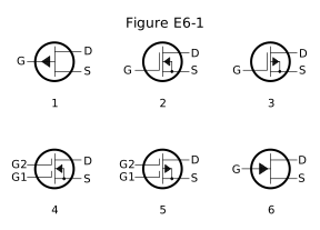
Figure E6-1 - A. 2
- B. 4
- C. 5
- D. 6
Show answer
B. 4
In Figure E6-1, a MOSFET symbol shows its gate as a line separated from the channel by a gap, representing the insulated gate. Symbol 4 has two separate gate leads (G1 and G2), and the arrow on its substrate connection points in toward the channel, which marks N-channel.
- A. Symbol 2 has the insulated gate and inward-pointing arrow of an N-channel MOSFET, but only one gate lead, so it is a single-gate device.
- C. Symbol 5 has two gate leads, but its arrow points out from the channel, which marks a P-channel dual-gate MOSFET.
- D. Symbol 6 has a single gate that touches the channel line with no gap and an arrow pointing in, which marks an N-channel junction FET.
E6A11
In Figure E6-1, which is the schematic symbol for a P-channel junction FET?
Figure E6-1 - A. 1
- B. 2
- C. 3
- D. 6
Show answer
A. 1
In Figure E6-1, a junction FET symbol has its gate lead connected directly to the channel line, with no insulating gap. The arrow on the gate points from P toward N material, so an arrow pointing out from the channel, as in symbol 1, marks a P-channel JFET.
- B. Symbol 2 has a gate separated from the channel by a gap and an inward-pointing arrow, which marks an N-channel MOSFET.
- C. Symbol 3 is P-channel (its arrow points out), but its gate is separated from the channel by a gap, which marks a MOSFET rather than a junction FET.
- D. Symbol 6 is a junction FET, but its arrow points in toward the channel, which marks N-channel.
E6A12
What is the purpose of connecting Zener diodes between a MOSFET gate and its source or drain?
- A. To provide a voltage reference for the correct amount of reverse-bias gate voltage
- B. To protect the substrate from excessive voltages
- C. To keep the gate voltage within specifications and prevent the device from overheating
- D. To protect the gate from static damage
Show answer
D. To protect the gate from static damage
A MOSFET's gate is insulated from the channel by a very thin oxide layer, which a static discharge can puncture. Zener diodes between the gate and the source or drain clamp the gate voltage to a safe level and conduct static charge away before it damages the oxide.
- A. Gate bias is set by the external circuit; the protective Zeners conduct only when the gate voltage exceeds a safe level.
- B. The vulnerable part of a MOSFET is the thin oxide insulating the gate, not the substrate.
- C. The Zeners do limit the gate voltage, but their purpose is to protect the gate oxide from static discharge; overheating comes from drain current and power dissipation, which they do not control.
E6B Diodes
E6B01
What is the most useful characteristic of a Zener diode?
- A. A constant current drop under conditions of varying voltage
- B. A constant voltage drop under conditions of varying current
- C. A negative resistance region
- D. An internal capacitance that varies with the applied voltage
Show answer
B. A constant voltage drop under conditions of varying current
When a Zener diode is reverse biased into breakdown, the voltage across it stays nearly constant over a wide range of current. This makes it useful as a voltage reference and as a simple voltage regulator.
- A. A Zener holds voltage, not current, nearly constant; a device that holds current constant is a current regulator diode.
- C. A negative resistance region is the characteristic of a tunnel diode, not a Zener diode.
- D. Internal capacitance that varies with applied voltage is the characteristic of a varactor diode.
E6B02
Which characteristic of a Schottky diode makes it a better choice than a silicon junction diode for use as a power supply rectifier?
- A. Much higher reverse voltage breakdown
- B. More constant reverse avalanche voltage
- C. Longer carrier retention time
- D. Lower forward voltage drop
Show answer
D. Lower forward voltage drop
A Schottky diode's metal-semiconductor junction has a lower forward voltage drop than a silicon PN junction, typically a few tenths of a volt compared with about 0.6 to 0.7 volts. In a power supply rectifier, a lower drop wastes less power as heat (P = forward voltage x current) and leaves more output voltage.
- A. Schottky diodes generally have lower reverse breakdown voltages than silicon junction diodes, not higher.
- B. A stable reverse breakdown (avalanche) voltage is what a Zener or avalanche diode provides; it is not the Schottky diode's advantage as a rectifier.
- C. Schottky diodes store very little charge, which lets them switch quickly; long carrier retention would be a disadvantage.
E6B03
What property of an LED's semiconductor material determines its forward voltage drop?
- A. Intrinsic resistance
- B. Band gap
- C. Junction capacitance
- D. Junction depth
Show answer
B. Band gap
In an LED, electrons crossing the junction fall across the semiconductor's band gap and give up that energy as light. A wider band gap means both higher-energy (shorter wavelength) light and a higher forward voltage, so a blue LED needs roughly 3 volts while a red LED needs roughly 2 volts.
- A. Resistance within the material adds a small voltage that rises with current, but the basic forward voltage is set by the band gap.
- C. Junction capacitance affects how fast an LED can switch, not its forward voltage.
- D. Junction depth is a manufacturing dimension; it does not set the forward voltage.
E6B04
What type of semiconductor device is designed for use as a voltage-controlled capacitor?
- A. Varactor diode
- B. Tunnel diode
- C. Silicon-controlled rectifier
- D. Zener diode
Show answer
A. Varactor diode
A varactor diode is designed to be used reverse biased as a voltage-controlled capacitor. The reverse voltage sets the width of the depletion region, which acts as the capacitor's dielectric: more reverse voltage widens it and lowers the capacitance. Varactors are used for electronic tuning.
- B. A tunnel diode is known for its negative resistance region, used in oscillators and amplifiers, not as a variable capacitor.
- C. A silicon-controlled rectifier is a switch that is turned on by a gate signal, not a variable capacitor.
- D. A Zener diode provides a constant voltage in reverse breakdown, not a controlled capacitance.
E6B05
What characteristic of a PIN diode makes it useful as an RF switch?
- A. Extremely high reverse breakdown voltage
- B. Ability to dissipate large amounts of power
- C. Reverse bias controls its forward voltage drop
- D. Low junction capacitance
Show answer
D. Low junction capacitance
A PIN diode has a wide intrinsic (undoped) layer between its P and N regions. With zero or reverse bias, that wide layer gives a very low junction capacitance, so the diode blocks RF well; with forward bias current, it conducts RF with low resistance. That pair of states makes it a good RF switch.
- A. Some PIN diodes do have high breakdown voltage, but switching comes from low capacitance when off and low resistance when forward biased.
- B. An RF switch should dissipate as little power as possible; PIN diodes are chosen for their low off-state capacitance, not for dissipating heat.
- C. Reverse bias does not control a forward voltage drop; in a PIN diode, the forward bias current controls its RF resistance.
E6B06
Which of the following is a common use of a Schottky diode?
- A. In oscillator circuits as the negative resistance element
- B. As a variable capacitance in an automatic frequency control circuit
- C. In power supplies as a constant voltage reference
- D. As a VHF/UHF mixer or detector
Show answer
D. As a VHF/UHF mixer or detector
Schottky diodes switch very quickly, because their metal-semiconductor junction stores very little charge, and they have low junction capacitance. These properties make them common as mixers and detectors at VHF, UHF and microwave frequencies.
- A. The negative resistance element in an oscillator is a tunnel diode or Gunn diode, not a Schottky diode.
- B. A variable capacitance for automatic frequency control is provided by a varactor diode.
- C. A constant voltage reference in a power supply is provided by a Zener diode.
E6B07
What causes a junction diode to fail from excessive current?
- A. Excessive inverse voltage
- B. Excessive junction temperature
- C. Insufficient forward voltage
- D. Charge carrier depletion
Show answer
B. Excessive junction temperature
Forward current through a diode dissipates power in the junction (forward voltage x current), which heats it. Too much current raises the junction temperature beyond its limit and permanently damages the semiconductor.
- A. Excessive inverse voltage destroys a diode by reverse breakdown, a different failure from excessive forward current.
- C. Insufficient forward voltage only means the diode does not conduct; it cannot cause the diode to fail.
- D. "Charge carrier depletion" is not a failure mechanism; a depletion region is a normal part of every PN junction.
E6B08
Which of the following is a Schottky barrier diode?
- A. Metal-semiconductor junction
- B. Electrolytic rectifier
- C. PIN junction
- D. Thermionic emission diode
Show answer
A. Metal-semiconductor junction
A Schottky barrier diode is formed by a junction between a metal and a semiconductor, rather than between P-type and N-type semiconductor. This junction gives it a low forward voltage and fast switching.
- B. An electrolytic rectifier uses metal electrodes in a chemical solution, not a metal-semiconductor junction.
- C. A PIN junction has P-type, intrinsic and N-type semiconductor layers, with no metal-semiconductor junction.
- D. A thermionic emission diode is a vacuum tube diode, in which a heated cathode emits electrons across a vacuum to a plate.
E6B09
What is a common use for point-contact diodes?
- A. As a constant current source
- B. As a constant voltage source
- C. As an RF detector
- D. As a high-voltage rectifier
Show answer
C. As an RF detector
A point-contact diode is formed where a fine wire touches a semiconductor crystal. The tiny contact area gives very low capacitance, so it works at high frequencies, and it is commonly used as an RF detector, as in the original crystal radio detector.
- A. A constant current source is built with a current regulator diode or transistor circuit, not a point-contact diode.
- B. A constant voltage source uses a Zener diode, not a point-contact diode.
- D. The tiny contact area of a point-contact diode handles only small currents and voltages; high-voltage rectifiers use large silicon junctions.
E6B10
In Figure E6-2, which is the schematic symbol for a Schottky diode?
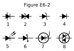
Figure E6-2 - A. 1
- B. 6
- C. 2
- D. 3
Show answer
B. 6
In Figure E6-2, the Schottky diode symbol is symbol 6: an ordinary diode triangle whose cathode bar ends in small hooks pointing in opposite directions, forming an S shape (for Schottky).
- A. Symbol 1 adds a curved line across the diode triangle; it does not have the S-shaped cathode bar that marks a Schottky diode.
- C. Symbol 2 shows two diode triangles pointing into a bracket-shaped bar; it does not have the S-shaped cathode bar that marks a Schottky diode.
- D. Symbol 3 has a cathode bar with its ends bent into a Z shape, which marks a Zener diode.
E6B11
What is used to control the attenuation of RF signals by a PIN diode?
- A. Forward DC bias current
- B. A variable RF reference voltage
- C. Reverse voltage larger than the RF signal
- D. Capacitance of an RF coupling capacitor
Show answer
A. Forward DC bias current
A PIN diode's resistance to RF depends on its forward DC bias current: more current fills the intrinsic layer with charge carriers and lowers its RF resistance. Varying the bias current therefore varies the attenuation, so a PIN diode can act as a current-controlled RF attenuator.
- B. A variable RF reference voltage is not used; the DC bias current sets the diode's RF resistance.
- C. A reverse voltage larger than the RF signal holds the diode fully off for maximum isolation; it does not vary the attenuation.
- D. Coupling capacitors pass RF and block DC; they do not control the attenuation.
E6C Digital ICs: families of digital ICs; gates; programmable logic devices
E6C01
What is the function of hysteresis in a comparator?
- A. To prevent input noise from causing unstable output signals
- B. To allow the comparator to be used with AC input signals
- C. To cause the output to continually change states
- D. To increase the sensitivity
Show answer
A. To prevent input noise from causing unstable output signals
Hysteresis gives a comparator two thresholds: once the output switches, the input must move back past a different threshold before it switches again. Noise riding on a slowly changing input near the threshold therefore cannot make the output chatter back and forth.
- B. Comparators can work with AC input signals without hysteresis; hysteresis addresses noise near the threshold.
- C. Continual changes of state are the chatter that hysteresis prevents; continual switching is what an oscillator does.
- D. Hysteresis deliberately reduces sensitivity to small input changes, because the input must move farther before the output switches back.
E6C02
What happens when the level of a comparator’s input signal crosses the threshold voltage?
- A. The IC input can be damaged
- B. The comparator changes its output state
- C. The reference level appears at the output
- D. The feedback loop becomes unstable
Show answer
B. The comparator changes its output state
A comparator compares an input voltage with a threshold (reference) voltage. When the input crosses the threshold, the output switches from one state to the other, for example from low to high.
- A. Crossing the threshold is normal operation; damage comes from exceeding the input voltage ratings.
- C. The reference level is an input that sets the threshold; the output switches between two output levels and does not reproduce the reference.
- D. Crossing the threshold is normal operation and does not make a feedback loop unstable; the output changes state.
E6C03
What is tri-state logic?
- A. Logic devices with 0, 1, and high-impedance output states
- B. Logic devices that utilize ternary math
- C. Logic with three output impedances which can be selected to better match the load impedance
- D. A counter with eight states
Show answer
A. Logic devices with 0, 1, and high-impedance output states
Tri-state logic outputs can be 0, 1, or a high-impedance state that effectively disconnects the output. This lets several devices share one bus line, with only one device enabled to drive it at a time.
- B. Tri-state outputs carry ordinary binary data; the third state disconnects the output rather than representing a third digit value.
- C. The high-impedance state disconnects the output; it is not one of three impedances chosen to match a load.
- D. A counter with eight states is a three-bit binary counter, unrelated to tri-state outputs.
E6C04
Which of the following is an advantage of BiCMOS logic?
- A. Its simplicity results in much less expensive devices than standard CMOS
- B. It is immune to electrostatic damage
- C. It has the high input impedance of CMOS and the low output impedance of bipolar transistors
- D. All these choices are correct
Show answer
C. It has the high input impedance of CMOS and the low output impedance of bipolar transistors
BiCMOS combines CMOS and bipolar transistors on one chip. The CMOS input stage has the high input impedance of an insulated MOS gate, and the bipolar output stage has a low output impedance that can drive heavy loads quickly.
- A. BiCMOS combines two transistor technologies, which makes it more complex to manufacture than standard CMOS, not cheaper.
- B. BiCMOS inputs are MOS gates, so the devices remain susceptible to electrostatic damage.
- D. Only the combination of CMOS input impedance and bipolar output impedance is an advantage; the claims about cost and static immunity are false.
E6C05
Which of the following digital logic families has the lowest power consumption?
- A. Schottky TTL
- B. ECL
- C. NMOS
- D. CMOS
Show answer
D. CMOS
A CMOS gate uses complementary pairs of transistors, one of which is always off in either output state, so almost no current flows except while the gate is switching. This gives CMOS a lower power consumption than the other families listed.
- A. Schottky TTL is a bipolar logic family that draws supply current continuously in both output states.
- B. ECL (emitter-coupled logic) keeps its transistors out of saturation for high speed and draws a large, steady current, so its power consumption is high.
- C. NMOS uses a load that draws current whenever the output is low; CMOS pairs complementary transistors so that one is always off.
E6C06
Why do CMOS digital integrated circuits have high immunity to noise on the input signal or power supply?
- A. Large bypass capacitance is inherent
- B. The input switching threshold is about twice the power supply voltage
- C. The input switching threshold is about half the power supply voltage
- D. Bandwidth is very limited
Show answer
C. The input switching threshold is about half the power supply voltage
A CMOS input switches at about half the power supply voltage. Noise must therefore move an input roughly halfway between the supply rails before it can cause a false logic change, which gives CMOS a large noise margin.
- A. CMOS ICs do not contain large bypass capacitance; designers add bypass capacitors externally.
- B. A threshold of twice the supply voltage could never be reached by the input, so the gate could never switch.
- D. CMOS logic can be quite fast; its noise immunity comes from where its switching threshold is, not from limited bandwidth.
E6C07
What best describes a pull-up or pull-down resistor?
- A. A resistor in a keying circuit used to reduce key clicks
- B. A resistor connected to the positive or negative supply used to establish a voltage when an input or output is an open circuit
- C. A resistor that ensures that an oscillator frequency does not drift
- D. A resistor connected to an op-amp output that prevents signals from exceeding the power supply voltage
Show answer
B. A resistor connected to the positive or negative supply used to establish a voltage when an input or output is an open circuit
A pull-up resistor connects a logic input or output to the positive supply, and a pull-down resistor connects it to the negative supply or ground. When the line is otherwise open, as with an open switch or an open-collector output that is off, the resistor holds it at a defined voltage instead of letting it float.
- A. Key clicks are reduced by shaping the rise and fall times of the keyed waveform, not with pull-up or pull-down resistors.
- C. Oscillator stability comes from stable components and good design; a pull-up or pull-down resistor does not prevent drift.
- D. An op-amp output cannot swing beyond its supply voltages in any case; a resistor on its output is not a pull-up or pull-down resistor.
E6C08
In Figure E6-3, which is the schematic symbol for a NAND gate?
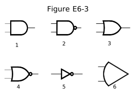
Figure E6-3 - A. 1
- B. 2
- C. 3
- D. 4
Show answer
B. 2
In Figure E6-3, symbol 2 is a NAND gate: the AND shape (flat input side and rounded output side) with a small circle, or bubble, at the output. The bubble means the AND result is inverted, so the output is low only when all inputs are high.
- A. Symbol 1 has the AND shape with no bubble at the output, so it is an AND gate.
- C. Symbol 3 has a curved input side and pointed output with no bubble, so it is an OR gate.
- D. Symbol 4 has the OR shape with a bubble at the output, so it is a NOR gate.
E6C09
What is used to design the configuration of a field-programmable gate array (FPGA)?
- A. Karnaugh maps
- B. Hardware description language (HDL)
- C. An auto-router
- D. Machine and assembly language
Show answer
B. Hardware description language (HDL)
An FPGA's configuration is described in a hardware description language (HDL), such as VHDL or Verilog. Software tools turn the HDL description into the configuration that sets up the FPGA's logic blocks and interconnections.
- A. Karnaugh maps are a manual method for simplifying small logic expressions; they are not practical for designing an FPGA configuration.
- C. An auto-router lays out the traces of a printed circuit board; it is not used to describe an FPGA's logic.
- D. Machine and assembly language program a microprocessor, which executes instructions in sequence; an FPGA is configured as hardware.
E6C10
In Figure E6-3, which is the schematic symbol for a NOR gate?
Figure E6-3 - A. 1
- B. 2
- C. 3
- D. 4
Show answer
D. 4
In Figure E6-3, symbol 4 is a NOR gate: the OR shape (curved input side and pointed output) with a small circle, or bubble, at the output. The bubble means the OR result is inverted, so the output is high only when all inputs are low.
- A. Symbol 1 has the AND shape (flat input side, rounded output) with no bubble, so it is an AND gate.
- B. Symbol 2 has the AND shape with a bubble at the output, so it is a NAND gate.
- C. Symbol 3 has the OR shape with no bubble at the output, so it is an OR gate.
E6C11
In Figure E6-3, which is the schematic symbol for the NOT operation (inversion)?
Figure E6-3 - A. 2
- B. 4
- C. 5
- D. 6
Show answer
C. 5
In Figure E6-3, symbol 5 is the inverter, which performs the NOT operation: a triangle with a single input and a small circle, or bubble, at its output. Its output is always the opposite of its input.
- A. Symbol 2 has two inputs and the AND shape with a bubble, so it is a NAND gate.
- B. Symbol 4 has two inputs and the OR shape with a bubble, so it is a NOR gate.
- D. Symbol 6 has two inputs and no bubble at its output; the inverter has one input and a bubble.
E6D Inductors and piezoelectricity: permeability, core material and configuration; transformers; piezoelectric devices
E6D01
What is piezoelectricity?
- A. The ability of materials to generate electromagnetic waves of a certain frequency when voltage is applied
- B. A characteristic of materials that have an index of refraction which depends on the polarization of the electromagnetic wave passing through it
- C. A characteristic of materials that generate a voltage when stressed and that flex when a voltage is applied
- D. The ability of materials to generate voltage when an electromagnetic wave of a certain frequency is applied
Show answer
C. A characteristic of materials that generate a voltage when stressed and that flex when a voltage is applied
Piezoelectric materials, such as quartz, produce a voltage when they are mechanically stressed and flex when a voltage is applied. This two-way link between mechanical motion and voltage lets a quartz crystal vibrate at a precise frequency in an oscillator or filter.
- A. Producing electromagnetic waves from an applied voltage describes an antenna driven by a transmitter, not piezoelectricity.
- B. An index of refraction that depends on polarization is birefringence, an optical property, not piezoelectricity.
- D. Producing a voltage from an incoming electromagnetic wave is what an antenna does; piezoelectricity links voltage to mechanical stress.
E6D02
What is the equivalent circuit of a quartz crystal?
- A. Series RLC in parallel with a shunt C representing electrode and stray capacitance
- B. Parallel RLC, where C is the parallel combination of resonance capacitance of the crystal and electrode and stray capacitance
- C. Series RLC, where C is the parallel combination of resonance capacitance of the crystal and electrode and stray capacitance
- D. Parallel RLC, where C is the series combination of resonance capacitance of the crystal and electrode and stray capacitance
Show answer
A. Series RLC in parallel with a shunt C representing electrode and stray capacitance
A quartz crystal is modeled as a series RLC circuit (the motional arm, representing the crystal's mechanical vibration) in parallel with a shunt capacitance from its electrodes, holder and strays. This gives the crystal both a series resonance and a slightly higher parallel resonance.
- B. A plain parallel RLC model leaves out the series motional arm, so it cannot produce the crystal's series resonance.
- C. A series RLC alone gives only series resonance; the electrode and stray capacitance is in parallel with the whole series arm, not combined with the motional capacitance.
- D. The model is a series RLC arm in parallel with a shunt capacitance, not a parallel RLC whose capacitance is a series combination.
E6D03
Which of the following is an aspect of the piezoelectric effect?
- A. Mechanical deformation of material due to the application of a voltage
- B. Mechanical deformation of material due to the application of a magnetic field
- C. Generation of electrical energy in the presence of light
- D. Increased conductivity in the presence of light
Show answer
A. Mechanical deformation of material due to the application of a voltage
The piezoelectric effect works both ways: mechanical stress on the material produces a voltage, and a voltage applied to the material makes it deform mechanically. The deformation caused by an applied voltage is what makes a quartz crystal vibrate in an oscillator.
- B. Deformation of a material by a magnetic field is magnetostriction, not the piezoelectric effect.
- C. Generating electrical energy from light is the photovoltaic effect, used in solar cells.
- D. Increased conductivity in the presence of light is photoconductivity.
E6D04
Why are cores of inductors and transformers sometimes constructed of thin layers?
- A. To simplify assembly during manufacturing
- B. To reduce power loss from eddy currents in the core
- C. To increase the cutoff frequency by reducing capacitance
- D. To save cost by reducing the amount of magnetic material
Show answer
B. To reduce power loss from eddy currents in the core
A changing magnetic field induces circulating currents, called eddy currents, in a conductive core, and those currents waste power as heat. Building the core from thin, insulated layers (laminations) breaks up the current paths, so eddy current losses are much smaller.
- A. Stacking thin laminations adds manufacturing steps; it is done to reduce eddy current loss, not to simplify assembly.
- C. Laminations reduce eddy current loss in the core; they are not used to reduce capacitance or raise a cutoff frequency.
- D. A laminated core contains nearly as much magnetic material as a solid core; the purpose is to reduce eddy currents, not cost.
E6D05
How do ferrite and powdered iron compare for use in an inductor core?
- A. Ferrite cores generally have lower initial permeability
- B. Ferrite cores generally have better temperature stability
- C. Ferrite cores generally require fewer turns to produce a given inductance value
- D. Ferrite cores are easier to use with surface-mount technology
Show answer
C. Ferrite cores generally require fewer turns to produce a given inductance value
Ferrite generally has much higher permeability than powdered iron. Because inductance rises with core permeability, a ferrite core needs fewer turns of wire to reach a given inductance.
- A. Ferrite generally has higher initial permeability than powdered iron, which is why it needs fewer turns.
- B. Powdered iron generally has better temperature stability than ferrite.
- D. Both materials are made in forms suitable for surface mounting; the general difference between them is permeability.
E6D06
What core material property determines the inductance of an inductor?
- A. Permittivity
- B. Resistance
- C. Reactivity
- D. Permeability
Show answer
D. Permeability
Permeability is a material's ability to support magnetic flux. Inductance is proportional to the permeability of the core, so a high-permeability core gives more inductance for the same coil than air or a low-permeability core.
- A. Permittivity is an electric property of a dielectric; it affects capacitance, not inductance.
- B. A core's resistance affects eddy current losses, not the inductance of the coil.
- C. "Reactivity" is a chemistry term, not a magnetic property of core materials.
E6D08
Which of the following materials has the highest temperature stability of its magnetic characteristics?
- A. Brass
- B. Powdered iron
- C. Ferrite
- D. Aluminum
Show answer
B. Powdered iron
Powdered iron cores keep their magnetic characteristics more stable over temperature than ferrite cores, though their permeability is lower. That stability makes powdered iron a good choice for tuned circuits and filters where the inductance must not drift.
- A. Brass is not a magnetic material; it is used in tuning slugs to reduce inductance, not as a magnetic core.
- C. Ferrite has higher permeability than powdered iron, but its magnetic characteristics change more with temperature.
- D. Aluminum is not a magnetic material, so it has no useful magnetic characteristics as a core.
E6D09
What devices are commonly used as VHF and UHF parasitic suppressors at the input and output terminals of a transistor HF amplifier?
- A. Electrolytic capacitors
- B. Butterworth filters
- C. Ferrite beads
- D. Steel-core toroids
Show answer
C. Ferrite beads
A ferrite bead slipped over a transistor lead adds a small inductance that becomes lossy at VHF and UHF. It absorbs energy at the high frequencies where parasitic oscillations occur, while having little effect at the HF operating frequency.
- A. Electrolytic capacitors have too much internal inductance to work at RF and are not used as parasitic suppressors.
- B. Butterworth describes a filter response with a flat passband; a Butterworth filter is not a device placed at transistor terminals to suppress parasitics.
- D. Steel-core toroids are not used as parasitic suppressors; a ferrite bead slips over a lead and adds loss at VHF and UHF.
E6D10
What is a primary advantage of using a toroidal core instead of a solenoidal core in an inductor?
- A. Toroidal cores confine most of the magnetic field within the core material
- B. Toroidal cores make it easier to couple the magnetic energy into other components
- C. Toroidal cores exhibit greater hysteresis
- D. Toroidal cores have lower Q characteristics
Show answer
A. Toroidal cores confine most of the magnetic field within the core material
In a toroid, the winding covers a closed ring of core material, so nearly all of the magnetic field stays inside the core. Little field leaks out to couple into nearby components, and outside fields have little effect on the toroid.
- B. The advantage is the opposite: a toroid confines its field, so it couples less with other components.
- C. Hysteresis depends on the core material, not its shape, and more hysteresis means more loss, which is not an advantage.
- D. Lower Q would be a disadvantage for most inductors; toroids are not chosen for it.
E6D11
Which type of core material decreases inductance when inserted into a coil?
- A. Ceramic
- B. Brass
- C. Ferrite
- D. Aluminum
Show answer
B. Brass
Brass is a nonmagnetic conductor. The coil's changing magnetic field induces eddy currents in a brass slug, and those currents create a field that opposes the coil's field, reducing the net flux and therefore the inductance. Brass slugs are used for this reason to tune coils downward in inductance.
- A. Ceramic is a nonmagnetic insulator, so it has little effect on inductance.
- C. Ferrite has high permeability, so inserting it into a coil increases the inductance.
- D. Aluminum is also a nonmagnetic conductor that can lower inductance through eddy currents, but brass is the material traditionally used for slugs that reduce inductance and is the answer this question expects.
E6D12
What causes inductor saturation?
- A. Operation at too high a frequency
- B. Selecting a core with low permeability
- C. Operation at excessive magnetic flux
- D. Selecting a core with excessive permittivity
Show answer
C. Operation at excessive magnetic flux
A magnetic core can carry only so much magnetic flux. When the current through the winding drives the flux beyond that limit, the core saturates: its permeability falls sharply, and the inductance drops.
- A. High frequency increases core losses, but saturation is caused by too much magnetic flux, not by frequency itself.
- B. A low-permeability core produces less flux for the same current, so it tolerates more current before saturating; saturation comes from excessive flux.
- D. Permittivity is an electric property of dielectrics; it has nothing to do with magnetic saturation.
E6E Semiconductor materials and packages for RF use
E6E01
Why is gallium arsenide (GaAs) useful for semiconductor devices operating at UHF and higher frequencies?
- A. Higher noise figures
- B. Higher electron mobility
- C. Lower junction voltage drop
- D. Lower transconductance
Show answer
B. Higher electron mobility
Electrons move much faster through gallium arsenide than through silicon (higher electron mobility). Faster carriers let GaAs transistors amplify at UHF and microwave frequencies with low noise.
- A. A higher noise figure would be a disadvantage; GaAs devices are valued for their low noise figure at UHF and microwave frequencies.
- C. GaAs has a wider band gap than silicon, so its junction voltage drop is higher, not lower.
- D. Lower transconductance means less gain for a given input voltage, which would be a disadvantage, not a reason to use GaAs.
E6E02
Which of the following device packages is a through-hole type?
- A. DIP
- B. PLCC
- C. BGA
- D. SOT
Show answer
A. DIP
A DIP (dual in-line package) has two rows of pins that pass through holes in the circuit board and are soldered on the other side, so it is a through-hole package.
- B. A PLCC (plastic leaded chip carrier) has J-shaped leads that are soldered to pads on the board surface, so it is a surface-mount package.
- C. A BGA (ball grid array) has an array of solder balls underneath that are soldered to pads on the board surface, so it is a surface-mount package.
- D. A SOT (small outline transistor) package is a small surface-mount package.
E6E03
Which of the following materials supports the highest frequency of operation when used in MMICs?
- A. Silicon
- B. Silicon nitride
- C. Silicon dioxide
- D. Gallium nitride
Show answer
D. Gallium nitride
Gallium nitride is a wide-band-gap compound semiconductor. Gallium nitride transistors combine fast electron transport with a high breakdown voltage, so gallium nitride MMICs work at high microwave frequencies and high power; of the materials listed, it supports the highest frequency of operation.
- A. Silicon devices are limited to lower frequencies than compound semiconductors such as gallium nitride, whose electrons move faster and which tolerate higher voltages.
- B. Silicon nitride is an insulator used in ICs for protective layers and capacitor dielectrics, not as the semiconductor that amplifies.
- C. Silicon dioxide is an insulator used in ICs for gate oxides and isolation, not as the semiconductor that amplifies.
E6E04
Which is the most common input and output impedance of MMICs?
- A. 50 ohms
- B. 300 ohms
- C. 450 ohms
- D. 75 ohms
Show answer
A. 50 ohms
Most MMICs are designed with input and output impedances of 50 ohms, the standard impedance of RF test equipment and coaxial cable systems. They can be connected in cascade without matching networks.
- B. 300 ohms is the impedance of common TV twin-lead, not the standard for MMICs.
- C. 450 ohms is the impedance of common window (ladder) line, not the standard for MMICs.
- D. 75 ohms is the standard for cable TV and video systems; most MMICs are designed for 50 ohms.
E6E05
Which of the following noise figure values is typical of a low-noise UHF preamplifier?
- A. 0.5 dB
- B. -10 dB
- C. 44 dBm
- D. -20 dBm
Show answer
A. 0.5 dB
Noise figure measures how much noise an amplifier adds, in dB; 0 dB would be a perfect, noiseless amplifier. A good low-noise UHF preamplifier adds very little noise, and a noise figure around 0.5 dB is typical.
- B. A noise figure cannot be negative; every real amplifier adds some noise, so the noise figure is always above 0 dB.
- C. dBm is a unit of power, not noise figure; 44 dBm is about 25 watts.
- D. dBm is a unit of power, not noise figure; -20 dBm is 10 microwatts.
E6E06
What characteristics of MMICs make them a popular choice for VHF through microwave circuits?
- A. The ability to retrieve information from a single signal, even in the presence of other strong signals
- B. Extremely high Q factor and high stability over a wide temperature range
- C. Nearly infinite gain, very high input impedance, and very low output impedance
- D. Controlled gain, low noise figure, and constant input and output impedance over the specified frequency range
Show answer
D. Controlled gain, low noise figure, and constant input and output impedance over the specified frequency range
MMICs (monolithic microwave integrated circuits) are amplifier blocks with a set, controlled gain, a low noise figure, and input and output impedances that stay constant, usually 50 ohms, across their rated frequency range. They can be dropped into a 50-ohm circuit with few external parts.
- A. Retrieving one signal in the presence of strong signals describes receiver selectivity and dynamic range, not a characteristic of MMICs.
- B. Extremely high Q and temperature stability describe quartz crystals and resonators; MMICs are broadband amplifiers.
- C. Nearly infinite gain, very high input impedance and very low output impedance describe an ideal operational amplifier, not an MMIC.
E6E07
What type of transmission line is often used for connections to MMICs?
- A. Miniature coax
- B. Circular waveguide
- C. Parallel wire
- D. Microstrip
Show answer
D. Microstrip
Microstrip is a circuit board trace running over a ground plane on the other side of the board, with its width chosen to give a controlled impedance, such as 50 ohms. It suits surface-mounted MMICs, which sit directly on the board.
- A. Coax may bring signals to a circuit board, but the connections to MMICs mounted on the board are usually microstrip traces.
- B. Circular waveguide is a large hollow pipe used to carry microwave signals over a distance; it is not used for connections to small IC packages.
- C. Parallel wire line is balanced line used for antenna feed lines; MMICs are unbalanced devices on a ground plane.
E6E08
How is power supplied to the most common type of MMIC?
- A. Through a capacitor and RF choke connected to the amplifier input lead
- B. MMICs require no operating bias
- C. Through a resistor and/or RF choke connected to the amplifier output lead
- D. Directly to the bias voltage (Vcc) lead
Show answer
C. Through a resistor and/or RF choke connected to the amplifier output lead
The most common type of MMIC has no separate power lead. DC is fed into the output lead through a resistor and/or RF choke, which supplies the bias while keeping the RF signal from being shorted to the power supply; a capacitor blocks the DC from the next stage.
- A. The bias is fed to the output lead, not the input; the input is connected through a DC blocking capacitor.
- B. MMICs contain transistors, which need DC operating bias like any amplifier.
- D. The most common type has no separate bias voltage lead; power reaches it through a resistor or RF choke on the output lead.
E6E09
Which of the following component package types have the least parasitic effects at frequencies above the HF range?
- A. TO-220
- B. Axial lead
- C. Radial lead
- D. Surface mount
Show answer
D. Surface mount
Surface-mount packages are small and have very short connections or none at all, so they add little stray inductance and capacitance. Above HF, these parasitic effects matter, so surface-mount parts behave closer to their nominal values.
- A. A TO-220 is a power package with long leads and a metal tab, which add more parasitic inductance and capacitance than a surface-mount part.
- B. Axial-lead components have a wire lead at each end, and the lead length adds parasitic inductance.
- C. Radial-lead components have wire leads from one end, and the lead length adds parasitic inductance.
E6E10
What advantage does surface-mount technology offer at RF compared to using through-hole components?
- A. Smaller circuit area
- B. Shorter circuit board traces
- C. Components have less parasitic inductance and capacitance
- D. All these choices are correct
Show answer
D. All these choices are correct
Surface-mount components are small and sit directly on the board, which saves circuit area, allows shorter traces between parts, and cuts the parasitic inductance and capacitance that leads add. All three listed advantages apply.
- A. Smaller circuit area is an advantage of surface-mount technology, but it is only one of the listed advantages.
- B. Shorter circuit board traces are an advantage of surface-mount technology, but they are only one of the listed advantages.
- C. Less parasitic inductance and capacitance is an advantage of surface-mount technology, but it is only one of the listed advantages.
E6E11
What is a characteristic of DIP packaging used for integrated circuits?
- A. Extremely low stray capacitance (dielectrically isolated package)
- B. Extremely high resistance between pins (doubly insulated package)
- C. Two chips in each package (dual in package)
- D. Two rows of connecting pins on opposite sides of package (dual in-line package)
Show answer
D. Two rows of connecting pins on opposite sides of package (dual in-line package)
DIP stands for dual in-line package: a rectangular IC package with two parallel rows of pins, one along each long side.
- A. DIP does not stand for "dielectrically isolated package," and its long leads give it more stray capacitance than smaller packages, not less.
- B. DIP does not stand for "doubly insulated package"; the name refers to its two rows of pins.
- C. The word dual refers to two rows of pins, not two chips; DIP stands for dual in-line package.
E6E12
Why are DIP through-hole package ICs not typically used at UHF and higher frequencies?
- A. Excessive dielectric loss
- B. Epoxy coating is conductive above 300 MHz
- C. Excessive lead length
- D. Unsuitable for combining analog and digital signals
Show answer
C. Excessive lead length
The pins of a DIP package and the internal connections to the chip are relatively long, and long leads add inductance and capacitance. At UHF and above, these parasitic effects are large enough to upset circuit operation.
- A. Dielectric loss in the package material is not what limits DIPs; the long leads are.
- B. The epoxy body of an IC remains an insulator at 300 MHz and above; it does not become conductive.
- D. DIP ICs can handle mixed analog and digital signals; the limitation at UHF is lead length.
E6F Electro-optical technology: photoconductivity; photovoltaic devices; optical sensors and encoders; optically isolated switching
E6F01
What absorbs the energy from light falling on a photovoltaic cell?
- A. Protons
- B. Photons
- C. Electrons
- D. Holes
Show answer
C. Electrons
In a photovoltaic cell, electrons in the semiconductor absorb the energy of incoming light. The absorbed energy frees them to move, and the cell's junction sweeps them out as an electric current.
- A. Protons are in the atomic nuclei and do not absorb light energy in a photovoltaic cell.
- B. Photons are the particles of light; they carry the energy that is absorbed, rather than absorbing it.
- D. Holes are the vacancies left behind when electrons are freed; they result from the absorption rather than doing it.
E6F02
What happens to photoconductive material when light shines on it?
- A. Resistance decreases
- B. Resistance increases
- C. Reflectivity increases
- D. Reflectivity decreases
Show answer
A. Resistance decreases
In a photoconductive material, light frees additional charge carriers, so the material conducts better and its resistance decreases. A photoresistor works this way: high resistance in the dark, lower resistance in light.
- B. Light frees more charge carriers, so resistance goes down, not up.
- C. Photoconductivity is a change in electrical conductivity, not in optical reflectivity.
- D. Photoconductivity is a change in electrical conductivity, not in optical reflectivity.
E6F03
What is the most common configuration of an optoisolator or optocoupler?
- A. A lens and a photomultiplier
- B. A frequency-modulated helium-neon laser
- C. An amplitude-modulated helium-neon laser
- D. An LED and a phototransistor
Show answer
D. An LED and a phototransistor
An optoisolator, or optocoupler, packages an LED and a phototransistor facing each other. The input current lights the LED, and the light turns on the phototransistor, so the signal crosses with no electrical connection between input and output.
- A. A photomultiplier is a vacuum tube that detects very faint light; optoisolators do not use one.
- B. A helium-neon laser is a gas laser, far too large for an optoisolator, which uses a small LED.
- C. A helium-neon laser is a gas laser, far too large for an optoisolator, which uses a small LED.
E6F04
What is the photovoltaic effect?
- A. The conversion of voltage to current when exposed to light
- B. The conversion of light to electrical energy
- C. The effect that causes a photodiode to emit light when a voltage is applied
- D. The effect that causes a phototransistor’s beta to decrease when exposed to light
Show answer
B. The conversion of light to electrical energy
The photovoltaic effect is the direct conversion of light into electrical energy: light absorbed at a semiconductor junction produces a voltage and can drive current through a load. Solar cells work this way.
- A. Light does not convert voltage into current; in the photovoltaic effect, light itself produces the voltage and current.
- C. A diode that emits light when a voltage is applied is an LED; that is the reverse of the photovoltaic effect.
- D. Light falling on a phototransistor produces base current that increases its collector current; there is no effect that decreases beta.
E6F05
Which of the following describes an optical shaft encoder?
- A. A device that detects rotation by interrupting a light source with a patterned wheel
- B. A device that measures the strength of a beam of light using analog-to-digital conversion
- C. An optical computing device in which light is coupled between devices by fiber optics
- D. A device for generating RTTY signals by means of a rotating light source
Show answer
A. A device that detects rotation by interrupting a light source with a patterned wheel
An optical shaft encoder has a wheel with a pattern of slots or marks that turns with the shaft and interrupts a light beam aimed at a light sensor. The resulting pulses show how far and in which direction the shaft has turned; many radios use one behind the tuning knob.
- B. Measuring the strength of a light beam with analog-to-digital conversion describes a digital light meter, not a shaft encoder.
- C. Coupling light between devices by fiber optics describes optical communication or computing, not a shaft encoder.
- D. RTTY signals are generated electronically by frequency-shift keying, not with a rotating light source.
E6F06
Which of these materials is most commonly used to create photoconductive devices?
- A. Polyphenol acetate
- B. Argon
- C. Crystalline semiconductor
- D. All these choices are correct
Show answer
C. Crystalline semiconductor
Photoconductive devices are made from crystalline semiconductors, such as cadmium sulfide or silicon, in which light frees charge carriers and lowers the resistance.
- A. Polyphenol acetate is not a material used to make photoconductive devices.
- B. Argon is an inert gas, used in some lamps and lasers; it is not photoconductive.
- D. Only crystalline semiconductor is used; the other two materials are not photoconductive device materials.
E6F07
What is a solid-state relay?
- A. A relay that uses transistors to drive the relay coil
- B. A device that uses semiconductors to implement the functions of an electromechanical relay
- C. A mechanical relay that latches in the on or off state each time it is pulsed
- D. A semiconductor switch that uses a monostable multivibrator circuit
Show answer
B. A device that uses semiconductors to implement the functions of an electromechanical relay
A solid-state relay uses semiconductors, often an optoisolator driving a transistor, triac or MOSFET output, to do the job of an electromechanical relay: a small control signal switches a separate load circuit, but with no moving contacts.
- A. A relay whose coil is driven by transistors is still an electromechanical relay with moving contacts.
- C. A mechanical relay that changes state and stays there each time it is pulsed is a latching relay.
- D. A monostable multivibrator produces a single timed pulse; it is not what defines a solid-state relay.
E6F08
Why are optoisolators often used in conjunction with solid-state circuits that control 120 VAC circuits?
- A. Optoisolators provide a low-impedance link between a control circuit and a power circuit
- B. Optoisolators provide impedance matching between the control circuit and power circuit
- C. Optoisolators provide an electrical isolation between a control circuit and the circuit being switched
- D. Optoisolators eliminate the effects of reflected light in the control circuit
Show answer
C. Optoisolators provide an electrical isolation between a control circuit and the circuit being switched
An optoisolator passes the control signal as light across a gap, with no electrical connection. This keeps the dangerous 120 VAC side electrically isolated from the low-voltage control circuit, protecting both the circuit and the operator.
- A. An optoisolator provides isolation, not a low-impedance link; a low-impedance connection would defeat its purpose.
- B. Optoisolators are not impedance-matching devices; their purpose is electrical isolation.
- D. The light path inside an optoisolator is sealed; it is not used to deal with reflected light.
E6F09
What is the efficiency of a photovoltaic cell?
- A. The output RF power divided by the input DC power
- B. The output in lumens divided by the input power in watts
- C. The open-circuit voltage divided by the short-circuit current under full illumination
- D. The relative fraction of light that is converted to current
Show answer
D. The relative fraction of light that is converted to current
The efficiency of a photovoltaic cell is the fraction of the light falling on it that it converts to electrical output. A cell that converts 20 percent of the incident light power to electrical power is 20 percent efficient.
- A. Output RF power divided by input DC power is the efficiency of an RF amplifier or transmitter, not a photovoltaic cell.
- B. Lumens per watt is the luminous efficacy of a light source, such as a lamp, not the efficiency of a photovoltaic cell.
- C. Open-circuit voltage divided by short-circuit current has units of ohms; it is a resistance, not an efficiency.
E6F10
What is the most common material used in power-generating photovoltaic cells?
- A. Selenium
- B. Silicon
- C. Cadmium sulfide
- D. Indium arsenide
Show answer
B. Silicon
Silicon is the most widely used material for power-generating photovoltaic cells, the solar cells used in panels for generating electricity.
- A. Selenium was used in early photocells and light meters, but it is not the common material for power-generating cells.
- C. Cadmium sulfide is commonly used in photoconductive cells (light-dependent resistors), not in power-generating photovoltaic cells.
- D. Indium arsenide is used in infrared detectors, not in power-generating photovoltaic cells.
E6F11
What is the approximate open-circuit voltage produced by a fully illuminated silicon photovoltaic cell?
- A. 0.5 volts
- B. 0.7 volts
- C. 1.1 volts
- D. 1.5 volts
Show answer
A. 0.5 volts
A fully illuminated silicon photovoltaic cell produces an open-circuit voltage of roughly half a volt. Because one cell gives well under a volt, solar panels connect many cells in series to reach useful voltages.
- B. 0.7 volts is the familiar forward voltage of a conducting silicon diode; the commonly cited figure for a silicon cell's open-circuit voltage is about 0.5 volts.
- C. 1.1 volts is far more than a single silicon cell produces.
- D. 1.5 volts is the voltage of a common alkaline battery cell, not a silicon photovoltaic cell.